Support QRP CoA Everywhere

Thursday 30 April 2009

FUCHS Antenna


This was discussed on GQRP a few weeks ago.


I thought I'd check and see if I had all the components to build it.


Well the answer is yes. So I then looked for a small enclosure and found one that I bought from Bowood Electronics (£1.50). The top was metal so I replaced that with the yellow rectangle a piece of FR4 double sided PCB with the copper removed.

I will add a little swtch so that the 10pF between the grounds can be disconnected.

HF DDS VFO


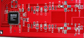
Decided to also build an older DDS VFO from AA0ZZ. I had an old red PCB from a purchase a while back (no components) so raided the component shelf and started to put that together.

So far my build looks like this:


The underneath... AD9854AST not the easiest to solder


I will use this one as bench top sig gen.


Wednesday 29 April 2009

GQRP Valve Day/Xtal post rigs

Click on either image to view larger.

"The Scrounger"


Capacitors on Xtal side are:


C1 Beehive trimmer


C2 100pF 500V silver mica


C3 0.02uF 500V ceramic disc.


Paraset


No C on xtal side of the Paraset except the gimmic wire wound couple times around the anode connection.

I am using these valve TX and the "cat meow" effect occured with the Scrounger (First one I built) and when I tried to use a HC49 crystal with a small lamp in series to reduce the current flowing through the crystal the meow was the result. The same settings with a HC6 4MHz crystal had just worked.
Suggested I try this:
But not sure I have the values needed.

Tuesday 28 April 2009

AA0ZZ IQPRO & LNA/LPF


Hopefully this is what mine will look like soon.

It started off like this:

It currently looks like this: Some components just placed some soldered, (click any of the following images to zoom in for a close up image)

Now all I have are soldered (except torroids and PIC's waiting for 40 pin sockets):


I started this after 'refinding' my collection of AD chip samples after putting it away before going to HB9 in 2007! Right now the build is waiting for an order from Farnell and Digikey for a number of the SMD components and for a collection of the Hittite switches from FDIM (Craig).

Many of the components I had in the component supplies/junk box. Used 1/4 w rather than 1/8w resistors as those were what I have.

Although I doubled up some 1206 resistors to make the necessary values.
(tested with a meter for the correct resistance afterwards)

Over the last few evenings I have been winding toroids for several projects, including this one and they are all now in separate plastic bags.


It was interesting working on everything from FT240-43 to T20-2 and most sizes in between. A lot of the homebrew bench is being cleaned up and the shack tidyed. To allow me to work on 'clean items' (XYL defined) I also have a new tool box containing many of the different sizes of enamelled copper wire. Which allows me to wind these. Hopefully I will work out all my extra toroid orders (this set is full) before FDIM.

On the DDS-VFO yahoo group list I noted the new project by Paul Blum, K9ARF using the LNA/LPF and a really neat looking enclosure.


I had an exchnage with Craig as I was not sure I had started the LNA/LPF correctly as I seemed to have more boards than needed:

Hi Dom,

Yes, it may be confusing. Just remember that there are 7 LNAs needed for the full complement.

One of them is a "bypass" section for 160 meters and it just has the switches connected by a piece of coax. (It is still activated by a wire from the control section, just like the other LNAs.)There are 5 LPFs.
Each LNA "break-off board" handles two LNAs and each LPF "break-off board" handles two LPFs.
To handle all bands, including 160 meters, here's what you need:
1) One Main board (with PICs)
2) One DDS board
3) One "main LNA/LPF board" containing one LNA/LPF control section, two LNAs, buffer (2N5109 section) on LNA board, two LPFs
4) Three additional LNA sections, two of them containing 4 LNAs and the third containing just the LNA "bypass" section for 160meters. No 2N5109 section on these.
5) Two additional LPF sections, one populated with two LPFs and one populated with one LPF.
Hope that helps.-Craig, AA0ZZ

Further exchnages confirmed:
The LNA connections are listed LNA mute LNA1 to LNA6 and LNA engage None, LNA1 to LNA6.
The LPF connections are listed LPF engage LPF1 to LPF6

Actually, there are only 5 LPFs so LPF1 through LPF5 are used the last pin is a spare - just in case...but unused now.

This is important if you want the bands/code to operate correctly, on the master control board you connect the 7th 160m LNA to "NONE" LNA engage, you connect the other 6 LNA to LNA1 to LNA6. And the LPF to LPF1 to LPF5.


The coax needs to run between Hittite pin 1 U4 and pin 3 U5. When looking for a good place for this, the closest pads of C1 and C7 seemed appropriate and then between them. However as Craig pointed out there is a pad on each side for this coax connection. Jc and Jd. (Center and ground on each.)

Look above the letters undermeath and you'll find the connections

.........Jc.......................................................Jd

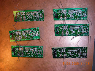
So as I have 4 of the boards with the control/lna/lpf section , the control sections on the top three boards and 1 LPF section are all surplus. You can snap them apart for a final assembly but keeping them together during the build makes it easier. Once done snap off the 3 control sections and one LPF section. On this picture that is the left most sections on top 3 boards and the upper right corner of the top board. (Click the image to zoom in) The picture is an early image as I was populating the SMD R and C from what I had.

Thursday 23 April 2009

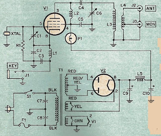
B2 Spyset Tx circuit

The TX circuit. Looking for the RX circuit... anyone?

Click it for a larger view.


Those pesky coil details of which don't seem to exist but found from an RSGB Bulletin (thanks Alan):

B2 Spyset TX

I spotted this was for sale on ebay. Quickly realised I could never afford to win the auction so asked if I could obtain photos, thanks Alan, here they are:


B2 Spyset

After starting off a build of a Paraset replica I picked up a few valves and though about all those stories you heard as a kid. Anyway wasn't long before I figured out the other tcvr used was a B2 spyset. I know I have some of the vavles and components for it so going to try an build a replica of that too.

The information I have so far is here and in newer posts.


Wednesday 22 April 2009

MiniVNA Extender PCB


Last April I bought a couple of these MiniVNA extender PCB from F1FRV but have not gotten around to building them yet. I will build one so the other is available.

Just to be clear.... as had a few enquiries about this.

I will not sell it, but I might swap it for something interesting.

As I homebrew a lot what PCB do you have for a project you never made (with components that are still available!)? A dip meter or some other bit of test kit. I am looking for a transformer impedance ratio meter... bit like this one http://www.siliconchip.com.au/cms/gallery/article.html?slideshow=0&a=101457&i=7

Monday 20 April 2009

MKARS 80m progress

Finished of the case and the CW adpater over w/e.

I bought an extra a case from Steve for the CW adapter and an other that holds a 12V SLA battery pack and a long wire ATU

Tuesday 14 April 2009

M1KTA ATS-3B Build


Opened the kit and printed off the assembly/operation manual.

And I finally started my ATS-3B build.

Resistors and inductors first...


As there will be plenty of reversing of the board during the construction stages I used a long 3mm bolt and nuts to support the board off the surface during construction. Rather than use a rotating vice.


This is almost straight down and it is almost impossible to see but the resistors and inductors have been soldered in place! 0805 and the tiny 0603 components. Started without aid of magnification. Hot iron and steady hand needed. If you click on the image and get the full size one you can see not the absolute neatest ever and I will clean off some of the excess solder!

I did not use the solder KD1JV (Steve) included as I already use 30swg solder and a temp controlled iron wih a 0.5mm tip (was 0.7mm but filed down a bit!).

Capacitor and surface mount IC's (you may notice I re arranged R5 too!)
(Note need to clean up the pads, you can clearly see too much solder on some and a little peak/point as the soldering iron was withdrawn)

Slanted view:


Reverse side


So far only taken a couple of hours soldering time. The 0603 resistors were not that bad, the difficult chip IS the DDS AD9834 as there is very little room. I used solder wick to separate three of the pins. The digital images on macro were excellent for seeing dry joints.

I think the difficult bit is now done :-)

The finished main board
Top

Bottom (L3 to fit after alignment)

The capacitors fitted to LPF (The green caps to be fitted after adjustment.)

The populated PCB

Monday 13 April 2009

QSBA


QSBA


Another kit from the shelf.

This one from KD1JV and it is the base station accessory for the ATS-3 series of rigs.

I have both an ATS-3 and ATS-3B kit and I am about to start of the ATS-3B version.

FCC-1 & FCC-2

FCC-1


FCC-2 (I have used a temporary knob just to confirm functionality)


Just finished the two NorCal kits FCC-1 and FCC-2 that I have had on the shelf for a while.

Exactly what I will do with them remains to be seen.

The FCC-1 as a standalone frequency counter is very useful.
The FCC-2 has the HF bands already coded into it with a selectable IF offset.